ECE 558/658 VLSI Design Principles
**IMPORTANT NOTE**: Notice that the numbers used in this example correspond to an older technology. As stated in the lab document, the example may not consider the worst case transition.
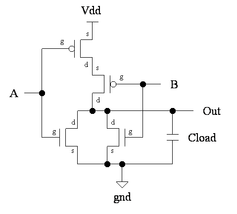
- Identify the worst-case transitions.
The worst case FALLING transition on OUT occurs when there is a RISING edge on A while B is held constant at logic 0. The worst case RISING transition on OUT occurs when there is a FALLING edge on A while B is held constant at logic 0.
- Determine the load capacitance Cload.
Suppose the specification is to be able to drive 16 minimum size inverters plus 100 fF of lumped wire capacitance. Then: Cinv = Cp + Cn
Cinv = Cox * L * (Wn + Wp)
Cinv = (6.03 fF/um^2) * (0.24 um) * (0.36 um + 1.08 um)
Cinv = 2.08 fF
Cload = 16 * Cinv + 100 fF
Cload = 16 * (2.08 fF) + 100 fF
Cload = 133 fF
- Determine the parasitic capacitance Cpara.
In the following example, the subscripts indicate the transistor and terminals. For example, in CgdnA, "gd" indicates the capacitor between the gate and drain terminals and "nA" indicates it's the NMOS transistor whose gate is connected to input A.
C = CgdnA + CdbnA + CgdnB + CdbnB + CgdpB + CdbpB + CgspB + CsbpB + CgdpA + CdbpA
We will assume that the drain and source of each transistor is geometrically identical, the two PMOS transistors are identical, and the two NMOS transistors are identical.
Cpara = 2*Cgdn + 2*Cdbn + 3*Cgdp + 3*Cdbp
Cpara = 2*(Cgdo*Wn) + 2*[Cj*Wn*Ls + Cjsw(2*Ls+Wn)] + 3*(Cgdo*Wp) + 3*[Cj*Wp*Ls + Cjsw(2*Ls+Wp)]
Cpara = 2*(0.63 fF/um)(Wn) + 2*[(1.92 fF/um^2)(Wn)(0.72 um) + (0.44 fF/um^2)(2*(0.72 um) + Wn)] + 3*(0.56 fF/um)(Wp) + 3*[(1.88 fF/um^2)(Wp)(0.72 um) + (0.37 fF/um)(2*(0.72 um) + Wp)]
Cpara = 1.26*Wn + 2.76*Wn + 1.27 + 0.88*Wn + 1.68*Wp + 4.06*Wp + 1.60 + 1.11*Wp
Cpara = 4.90*Wn + 6.85*Wp + 2.87
- Find Ctotal, the sum of Cload and Cpara.
Ctotal = Cpara + Cload
Ctotal = 4.90*Wn + 6.85*Wp + 2.87 + 133
Ctotal = 4.90*Wn + 6.85*Wp + 136
- Compute the total current required to switch all of this capacitance by 1/2 Vdd (= 1.25 V) in the required amount of time (say, 500 ps).
I = Ctotal * dV/dt
I = (4.90*Wn + 6.85*Wp + 136 fF) * (1.25 V) / (500 ps)
I = 1.23E-5*Wn + 1.71E-5*Wp + 3.40E-4
- Assuming operation in the saturation region, compute the current in the NMOS transistor during the worst-case FALLING edge on OUT. Then set this current equal to the capacitor current.
I = 0.5 * kn' * (Wn / L) * (Vgs - Vt)^2
I = 0.5 * (275E-6) * (Wn / 0.24 um) * (2.5 - 0.43)^2
I = 2.45E-3*Wn
1.23E-5*Wn + 1.71E-5*Wp + 3.40E-4 = 2.45E-3*Wn
2.44E-3*Wn - 1.71E-5*Wp = 3.40E-4
- Compute the current in the PMOS transistors during the worst-case RISING edge on OUT. Be sure to double the channel length because we're modeling them as two resistors in series. Then set this current equal to the capacitor current.
I = 0.5 * kp' * (Wp / L) * (Vgs - Vt)^2
I = 0.5 * (96E-6) * (Wp / 0.48 um) * (2.5 - 0.62)^2
I = 3.53E-4*Wp
1.23E-5*Wn + 1.71E-5*Wp + 3.40E-4 = 3.53E-4*Wp
3.36E-4*Wp - 1.23E-5*Wn = 3.40E-4
- Solve the two equations for Wn and Wp.
2.44E-3*Wn - 1.71E-5*Wp = 3.40E-4
Wn = 7.01E-3*Wp + 0.14
3.36E-4*Wp - 1.23E-5*Wn = 3.40E-4
3.36E-4*Wp - 1.23E-5*(7.01E-3*Wp + 0.14) = 3.40E-4
3.36E-4*Wp = 3.42E-4
Wp = 1.02 um
Wn = 7.01E-3*Wp + 0.14
Wn = 7.01E-3*1.02 + 0.14
Wn = 0.15 um
- Sanity check your answers.
In this process, we expect the PMOS device of an inverter to be ~3x the size of the NMOS device due to the difference in mobility between electrons and holes. In the NOR gate, there are 2 PMOS devices in series, so we would expect each one to be ~6x the size of the NMOS device. Thus, our answers have approximately the right ratio. However, the minimum device width in this process is 0.36 um, so we have to upsize the NMOS devices to be at least that large. While this increases the parasitic capacitances, it increases the current drive capability even more, so the falling transition will be much faster than required. We should not upsize the PMOS devices proportionally, however, because they are already large enough to satisfy our rising transition speed requirement.