|
![]()
|
|
|
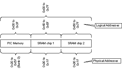
Lab InstructionsIn this lab, the PIC will be connected to external memory (SRAM). You will use simplified version of the PIC-PLD bus from Lab 2 to communicate with the PLD, which in turn manages the control signals for the SRAM. For the demo, you need to write a memory test program that can verify the correct operation of any range of memory locations in the virtual address space. The physical memory consists of PIC-internal memory and two external SRAM chips (see Figure).
TasksFor this lab you must complete the following tasks. 1. This VT220 interface should query the user for the start address of memory test (“Enter start address [0x00..0x7f]:”), the end address (“enter end address [0x00..0x7f]:”), and the 8-bit test pattern (“enter test pattern [0x00..0xff]:”). You may use polling (easier) or interrupts (for those who don’t find enough challenges in this project already) for reading from the serial port. It is required that you use the “advanced string printing” method with the RETLW instruction discussed in class. Your program must check the input for correctness (i.e., start address ≤ end address). If incorrect values are entered, you may just jump to the beginning of the input routine and start over (no error message required). 2.
The memory test will work as follows: You will test each
memory location in the range with eight patterns. These patterns are the input
pattern rotated left 0-7 times. You should first write the first pattern to all
memory locations within the range, then read them and verify correctness (do not
write, read, and check them one-by-one). Then repeat with the second through
eighth pattern. 3. For testing internal PIC memory (virtual address 0x00 to 0x3f), you should use indirect addressing as discussed in class. 4.
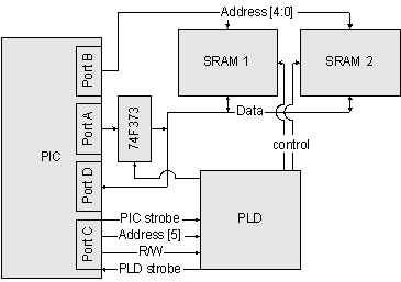
For the interface to the two
HM6264B SRAM chips, you should
set up the PLD to handle the control signals for the SRAM. The address and data
values are transferred directly (i.e., not via the PLD) between PIC and SRAM
(see Figure), except for addr[5], which is used to select between the SRAM chips
(partial address decoding). 5. To test your system, make sure the test runs without errors. Then introduce errors by disconnecting data wires (or pulling them to ground via 4.7k resistor). You will probably not be able to create errors by disconnecting address wires (why?). DemoDuring the demo, your PIC should perform the memory test robustly for any range of addresses and test pattern. I will test the correctness by pulling various address and data wires from the SRAM to verify that the test fails and prints the expected failure messages. You should also set up your lab to show the SRAM transactions on a logic analyzer (or show printouts). You do not need to show the PIC–PLD interactions. Getting StartedOne possible approach to implementing this lab is the following:
Lab ReportThe lab report guidelines are the same as for previous labs. Your report should include a schematics and a logic analyzer printout of SRAM read and write transactions. It is not required show PIC–PLD transactions. |
|