Two Bit Error Correction and Three Bit Error Detection Scheme with Minimal Latency
Overview
This page describes an error detection and correction scheme which:
To achieve low latency, a separate data path and control path were developed, and the number and type of check bits was changed from the traditional approach used for error detection and correction. While the traditional approach uses one monolithic check matrix and requires the control path to wait for the data path computations, the approach here is to detect the error type (i.e. no error, single, double, or triple-bit error) using two fast SEC/DED codes. This way the error type can be detected well ahead of the double-bit correction logic to complete. The primary drawback to this scheme is that the number of check bit is more than the minimum required.
Description
The heart of the scheme is the check matrix, which is made up of the following components:
The scheme developed works for any combination of data or check bit errors. It will detect, for example, 2 data bits and 1 check bit in error. Likewise, it will detect (or ignore) 3 check bits in error.
Instead of a monolithic check matrix with a Hamming distance of 5 (needed for 2-bit correction, distance = 2d+1 for d bits corrected), the two sub-matrices both have minimum distance of 4. Both are capable of correcting single-bit errors and detecting double-bit errors.
The number of check bits is 16, which is well above 11, the minimum required. A goal of 16 check bits was arrived at by rounding up to the next byte boundary (the minimum of 11 bits needed was rounded up to 16). This relaxation, although potentially very costly for a memory of custom width, has no impact when standard memory devices are used (which have byte granularity). The benefit of this relaxation was that it permitted the control logic to be driven strictly by low latency circuits, as described in more detail in the "A More Realistic Block Diagram of Decode Circuit" and "Control Logic" sections below.
Check Matrix
|
Data Bits |
ck_A |
Par_B |
ck_A |
||||||||||||||||||||||||||||||||||||||||||||
| D00 | D01 | D02 | D03 | D04 | D05 | D06 | D07 | D08 | D09 | D10 | D11 | D12 | D13 | D14 | D15 | D16 | D17 | D18 | D19 | D20 | D21 | D22 | D23 | D24 | D25 | D26 | D27 | D28 | D29 | D30 | D31 | P01 | P02 | P03 | P04 | P05 | P06 | P07 |
P08 |
P09 | P10 | P11 | P12 | P13 | P14 | P15 | P16 |
|
1 |
1 |
1 | 1 | 1 | 1 | 1 | 1 | 1 | 1 | 1 | 1 | 1 | 1 | 1 | |||||||||||||||||||||||||||||||||
| 1 | 1 | 1 | 1 | 1 | 1 | 1 | 1 | 1 | 1 | 1 | 1 | 1 | 1 | 1 | |||||||||||||||||||||||||||||||||
| 1 | 1 | 1 | 1 | 1 | 1 | 1 | 1 | 1 | 1 | 1 | 1 | 1 | 1 | 1 | |||||||||||||||||||||||||||||||||
| 1 | 1 | 1 | 1 | 1 | 1 | 1 | 1 | 1 | 1 | 1 | 1 | 1 | 1 | 1 | |||||||||||||||||||||||||||||||||
| 1 | 1 | 1 | 1 | 1 | 1 | 1 | 1 | 1 | 1 | 1 | 1 | 1 | 1 | 1 | |||||||||||||||||||||||||||||||||
| 1 | 1 | 1 | 1 | 1 | 1 | 1 | 1 | 1 | 1 | 1 | 1 | 1 | 1 | ||||||||||||||||||||||||||||||||||
| 1 | 1 | 1 | 1 | 1 | 1 | 1 | 1 | 1 | 1 | 1 | 1 | 1 | 1 | ||||||||||||||||||||||||||||||||||
| 1 | 1 | 1 | 1 | 1 | 1 | 1 | 1 | 1 | |||||||||||||||||||||||||||||||||||||||
| 1 | 1 | 1 | 1 | 1 | 1 | 1 | 1 | 1 | 1 | 1 | 1 | ||||||||||||||||||||||||||||||||||||
| 1 | 1 | 1 | 1 | 1 | 1 | 1 | 1 | 1 | 1 | 1 | 1 | ||||||||||||||||||||||||||||||||||||
| 1 | 1 | 1 | 1 | 1 | 1 | 1 | 1 | 1 | 1 | 1 | 1 | 1 | |||||||||||||||||||||||||||||||||||
| 1 | 1 | 1 | 1 | 1 | 1 | 1 | 1 | 1 | 1 | 1 | 1 | 1 | |||||||||||||||||||||||||||||||||||
| 1 | 1 | 1 | 1 | 1 | 1 | 1 | 1 | 1 | 1 | 1 | 1 | 1 | 1 | ||||||||||||||||||||||||||||||||||
| 1 | 1 | 1 | 1 | 1 | 1 | 1 | 1 | 1 | 1 | 1 | 1 | 1 | |||||||||||||||||||||||||||||||||||
| 1 | 1 | 1 | 1 | 1 | 1 | 1 | 1 | 1 | 1 | 1 | 1 | 1 | |||||||||||||||||||||||||||||||||||
| 1 | 1 | 1 | 1 | 1 | 1 | 1 | 1 | 1 | 1 | 1 | 1 | 1 | 1 | ||||||||||||||||||||||||||||||||||
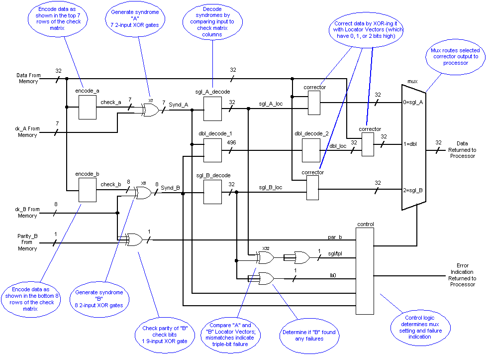
Block Diagram of the Decode Circuit with Comments
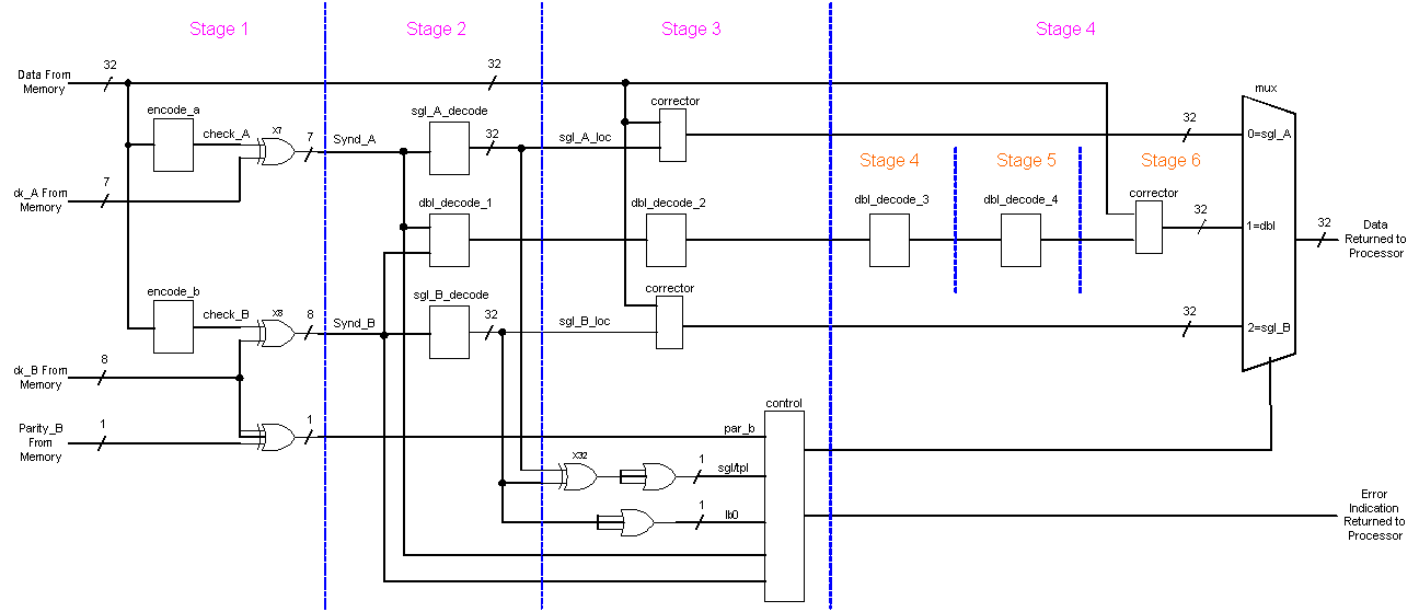
A More Realistic Block Diagram of Decode Circuit
The block diagram shown above is notional only. The dbl_decode_1 block contains 496 AND gates (32 items taken 2 at a time) which present around 150 to 200 loads on each of the syndrome signals (Synd_A and Synd_B). In addition, there are 32 OR gates in the dbl_decode_2 block, each of which has 31 inputs. These high fan-in and fan-out circuits will have timing problems during logic implementation. Since the circuits are combinational, the logic can be split over several clock cycles. The block diagram below shows the additional pipeline stages (i.e. pipeline registers at intersections with the blue lines) needed for a more realistic implementation. Since the control logic can determine what kind of error occurred before the results from the double-bit decode is available, it is capable of returning the no-correction or single-bit correction data with little penalty over a single-bit-only error correction circuit. Obviously, the control logic must have some control over the timing of returned data if it needs to wait (albeit rarely) for the corrected double-bit error data.
Control Logic
One of the requirements for a low-latency circuit is that the inputs to the control circuit not depend on the results of the high-latency (double bit locator) circuits. Thus, the control logic is designed to compute the error type using the following information:
To detect the type of error that has occurred, the control logic takes advantage of the fact that the two single-bit syndromes will both have an even number of bits high for a double-bit error. The following table, which shows the input values for error combination cases for 0, 1, 2, and 3 bit errors, was generated based on this fact. This table was used to create the control logic in the javascript code. Note that some error combinations do not require corrections (i.e. errors in the check bits only), so these errors are "ignored".
|
Bit Errors |
Case |
Error Combination |
1’s in Synd_a |
1’s in Synd_b |
par_b |
sgl/tpl |
lb0 |
Response Ignore/Correct/Detect |
Comments |
|
0 |
0 |
None |
0 |
0 |
|
|
|
|
|
|
1 |
1a |
Single check bit in ck_a/b |
1/0 |
0/1 |
|
|
|
|
|
|
1b |
Single data bit |
3 |
3 |
|
|
|
|
|
|
|
1c |
par_b bit |
0 |
0 |
|
|
|
|
||
|
2 |
2a |
Two check bits in ck_a/b |
2/0 |
0/2 |
|
|
|
|
|
|
2b |
Two check bits (1 each ck_a and ck_b) |
1 |
1 |
|
|
|
|
||
|
2c |
One ck_a and par_b |
1 |
0 |
|
|
|
Ignore |
||
|
2d |
One ck_b and par_b |
0 |
1 |
|
|
|
|
||
|
2e |
Single data and par_b |
3 |
3 |
|
|
|
|
|
|
|
2f |
Single data with overlapping ck_a/b |
2/3 |
3/2 |
|
|
|
|
|
|
|
2g |
Single data with non-overlapping ck_a/b |
4/3 |
3/4 |
|
|
|
|
|
|
|
2h |
Two data bits |
2,4,6 |
2,4,6 |
|
|
|
|
|
|
|
3 |
3a |
Three ck_a/b bits |
3/0 |
0/3 |
|
|
|
|
|
|
3b |
One ck_a, two ck_b |
1 |
2 |
|
|
|
|
||
|
3c |
Two ck_a, one ck_b |
2 |
1 |
|
|
|
|
||
|
3d |
Two ck_a, par_b |
2 |
0 |
|
|
|
|
||
|
3e |
Two ck_b, par_b |
0 |
2 |
|
|
|
|
||
|
3f |
One ck_a, one ck_b, par_b |
1 |
1 |
|
|
|
|
||
|
3g |
One data bit, two overlapping ck_a/b |
1/3 |
3/1 |
|
|
|
|
||
|
3h |
One data bit, one each over/non-over ck_a/b |
3/3 |
3/3 |
|
|
|
|
||
|
3i |
One data bit, two non-overlapping ck_a/b |
5/3 |
3/5 |
|
|
|
|
||
|
3j |
One data bit, one ck_a, one ck_b |
2,4 |
2,4 |
|
|
|
Detect |
||
|
3k |
One data bit, one ck_a, par_b |
2,4 |
3 |
|
|
|
Detect |
||
|
3l |
One data bit, one ck_b, par_b |
3 |
2,4 |
|
|
|
Detect |
||
|
3m |
Two data bits, ck_a |
1,3,5,7 |
2,4,6 |
|
|
|
Detect |
||
|
3n |
Two data bits, ck_b |
2,4,6 |
1,3,5,7 |
|
|
|
Detect |
||
|
3o |
Two data bits, par_b |
2,4,6 |
2,4,6 |
|
|
|
Detect |
||
|
3p |
Three data bits, resulting in unused syndromes |
3 |
3 |
|
|
|
Detect |
||
|
3q |
Three data bits |
0,1,3,5,7,9 |
0,1,3,5,7,9 |
|
|
|
Detect |
Response to Higher-Order Bit-Errors
The scheme's response to higher-order bits errors for all error combinations up to 7 bits was simulated with the results shown in the table below. In general, about half of the even-bit-errors are detected, and about 90% of the odd-bit-errors are detected.
|
|
Response |
|||
|
Correct/Ignore |
Detected |
Undetected |
Total |
|
|
Single |
100% |
0% |
0% |
100% |
|
Double |
100% |
0% |
0% |
100% |
|
Triple |
6.6% |
93.4% |
0% |
100% |
|
Four |
1.3% |
49.1% |
49.6% |
100% |
|
Five |
0.1% |
93.1% |
6.8% |
100% |
|
Six |
0.0% |
57.1% |
42.9% |
100% |
|
Seven |
0.0% |
91.7% |
8.3% |
100% |